
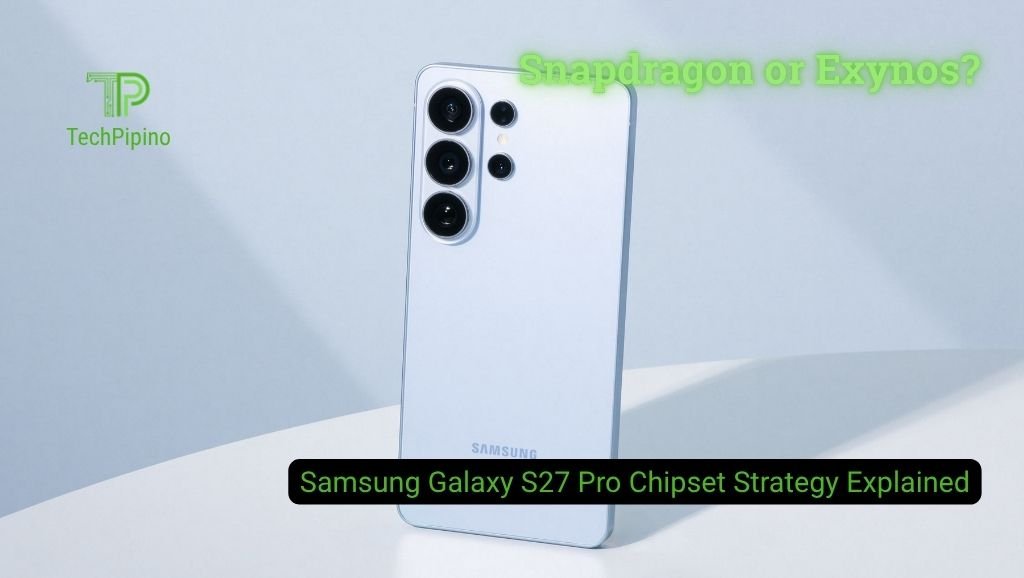
Samsung is solidifying its hardware roadmap for the upcoming Galaxy S27 series, confirming that the Galaxy S27 Pro will utilize the Exynos 2700 chipset across most global markets. This decision highlights a clear architectural divergence between the Pro and the premium Ultra model, which is slated to feature the Snapdragon Elite chip globally.
Architectural Shifts in the Exynos 2700
The Exynos 2700 represents a transition to Samsung’s SF2P manufacturing node. This process node is engineered to provide a 26% reduction in power consumption and a 15% increase in clock speeds compared to the SF2 node used in the Exynos 2600.
Beyond the node transition, Samsung is moving away from the conventional Package-on-Package design. The new Side-by-Side layout connects the DRAM and the chipset via a silicon interposer. In traditional stacked configurations, heat from the silicon die must dissipate through the memory layer before reaching the cooling solution. By placing components laterally, the thermal resistance between the heat-generating die and the cooling block is reduced, facilitating more consistent sustained performance.
Performance and Market Segmentation
The integration of the Exynos 2700 in the Galaxy S27 Pro, alongside the vanilla Galaxy S27 and S27+ models, underscores a strategic segmentation. North American markets, and potentially others, will continue to receive the Snapdragon Elite platform. Early benchmark data for the Exynos 2700 requires cautious interpretation, as initial test samples have operated at reduced clock frequencies—often hovering around 2.88GHz—compared to the rumored 4.2GHz peak capability for the ARM C2 Ultra cores.
While the S27 Pro shares several camera modules with the Ultra, this chipset differentiation confirms the device is not positioned as a compact version of the flagship Ultra. Instead, it occupies a distinct performance tier defined by regional availability and localized silicon optimization.
Quick Specs: Exynos 2700
| Parameter | Specification |
| Process Node | Samsung SF2P |
| Layout | Side-by-Side (DRAM/Chipset) |
| Target Architecture | ARM C2 Ultra Core |
| Efficiency Gain | 26% vs SF2 (Exynos 2600) |
| Reported Max Clock | 4.2GHz |
Why It Matters
The shift to a side-by-side memory layout is an acknowledgment that thermal management is the primary bottleneck for mobile sustained performance. By optimizing the physical architecture to lower the heat transfer path, Samsung is attempting to mitigate the thermal throttling often associated with dense chip designs. This strategy suggests a prioritization of efficiency and long-term thermal stability over raw, short-burst performance, which remains the domain of the Snapdragon-equipped Ultra variant.
FAQ
Will the Galaxy S27 Pro use a Snapdragon chip?
Only in select regions like North America. Most global markets will receive the Exynos 2700 version.
What is the advantage of the Side-by-Side layout?
It improves thermal management by allowing the chipset to connect directly to the cooling block rather than transferring heat through the stacked DRAM.
Is the Exynos 2700 faster than the Snapdragon Elite?
The two chips serve different market segments, with the Snapdragon Elite configured for the global Ultra model and the Exynos 2700 for the Pro, vanilla, and Plus models.
What is the manufacturing process for the Exynos 2700?
It is manufactured on Samsung’s SF2P node, designed for 26% improved power efficiency over previous generations.


